|
|

|
|
| Partname: | MAX9160AEUI |
| Description: | 3.0 V to 3.6 V, LVDS or LVTTL/LVCMOS input to 14 LVTTL/LVCMOS output clock driver |
| Manufacturer: | Maxim Integrated Products |
| Package: | TSSOP |
| Pins: | 28 |
| Oper. temp.: | -40 to 85 |
| Datasheet: | PDF (348K).
Click here to download *) |
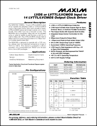
The MAX9160 125MHz, 14-port LVTTL/LVCMOS clock driver repeats the selected LVDS or LVTTL/LVCMOS input on two output banks. Each bank consists of seven LVTTL/LVCMOS series terminated outputs and a bank enable. The LVDS input has a fail-safe function. The MAX9160 has a propagation delay that can be adjusted using an external resistor to set the bias current for an internal delay cell. The LVTTL/LVCMOS outputs feature 200ps maximum output-to-output skew and 100ps maximum added peak-to-peak jitter. The MAX9160 is designed to operate with a 3.3V supply voltage over the extended temperature range of -40C to +85C. This device is available in 28-pin exposed- and nonexposed-pad TSSOP and 32-lead 5mm x 5mm QFN packages. |
|
Click here to download MAX9160AEUI Datasheet*) |
 |
| *)Datasheets downloading from ChipDocs is only for our members (paid service). REGISTER NOW for your membership. |
|
|
|

