|
|

|
|
| Partname: | BM29F040 |
| Description: | 4 megabit 5 volt sector erase CMOS flash memory |
| Manufacturer: | Winbond Electronics |
| Package: | P-DIP32 |
| Pins: | 32 |
| Oper. temp.: | -55 to 125 |
| Datasheet: | PDF (196K).
Click here to download *) |
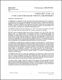
The BM29F040 is a 4 Megabit, 5.0 Volts only Flash memory device organized as 512K x 8 bits each. The BM29F040 is offered in an Industry standard 32-pin package which is backward compatible to 1 Megabit and also pin compatible to EEPROMs. The device is offered in PDIP, PLCC and TSOP packages. The device is designed to be programmed and erased in system with the standard system 5 Volt Vcc supply. An external 12.0 Volts Vpp is not required for program and erase operation. The device can also be reprogrammed in standard EPROM programmers. The BM29F040 offers access times between 70 to 150 nS. The device has separate chip enable ( CE ), write enable ( WE ) and output enable ( OE ) controls to eliminate bus contention. BMI flash memory technology reliably stores memory information even after 100,000 erase and program cycles. The BMI proprietary cell technology enhances the programming speeds and eliminates over erase problems seen in the classical ETOXTM type of Flash cell technologies. The combination of cell technology and internal circuit design techniques give reduced internal electrical fields and this provides improved reliability and endurance. The BM29F040 is entirely pin and command set compatible to the JEDEC standard 4 Megabit EEPROM. The commands are written to the Command State machine using standard microprocessor write timings. The internal Programming and Erase Algorithms are automatically implemented based on the input commands. The BM29F040 is programmed by executing the program command sequence. This will start the internal automatic program Algorithm that times the program pulse width and also verifies the proper cell margin. Erase is accomplished by executing the erase command sequence. The internal Power Switching State Machine automatically executes the algorithms and generates the necessary voltages and timings for the erase operation. The program and erase verify is also done internally and proper margin testing is automatically performed. This scheme unburdens the microprocessor or microcontroller from generating the program and erase algorithms by controlling all the necessary timings and voltages. The entire memory is typically erased in 1.5 seconds. No preprogramming is necessary in this technology. |
|

Click here to download BM29F040 Datasheet*) |
 |
| *)Datasheets downloading from ChipDocs is only for our members (paid service). REGISTER NOW for your membership. |
|
|
|

