|
|

|
|
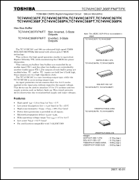
| Partname: | TC74VHC368FK |
| Description: | Hex Bus Buffer |
| Manufacturer: | Toshiba |
| Datasheet: | PDF (268K).
Click here to download *) |
They contain six buffers; four buffers are controlled by an enable input ( G1 ), and the other two buffers are controlled by another enable input ( G2 ). The outputs of each buffer group are enabled when G1 and/or G2 inputs are held low; if held high, these outputs are in a high impedance state. The TC74VHC367 is a non-inverting output type, while the TC74VHC368 is an inverting output type. An input protection circuit ensures that 0 to 5.5 V can be applied to the input pins without regard to the supply voltage. This device can be used to interface 5 V to 3 V systems and two supply systems such as battery back up. This circuit prevents device destruction due to mismatched supply and input voltages. |
|
Click here to download TC74VHC368FK Datasheet*) |
 |
| *)Datasheets downloading from ChipDocs is only for our members (paid service). REGISTER NOW for your membership. |
|
|
|

