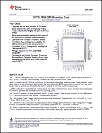
The DLPA200 is designed to be used as a part of a complete DLP chipset. A DLP chipset typically consists of a DMD, a DMD Controller, DMD Controller Firmware, and the DMD Micromirror Driver. Within a chipset, the DLPR200 is responsible for generating micromirror clocking pulses. These clocking pulses (also referred to as micromirror reset pulses) are what cause the DMD micromirrors to switch from one binary landed state to another (as dictated by the binary contents of the DMD CMOS memory array). A DMD Controller is responsible for writing data to the DMD CMOS memory array, and then commanding the DLPR200 to generate the required micromirror clocking pulses. The DLPA200 consists of three functional blocks: A High-Voltage Power Supply function, a DMD Micromirror Clock Generation function, and a Serial Communication function. The High-Voltage Power Supply function generates three specialized voltage levels: VBIAS (19 to 28 V), VRESET (19 to 28 V), and VOFFSET (4.5 to 10 V). The Micromirror Clock Generation function uses the three voltages generated by the High-Voltage Power Supply function to create the sixteen micromirror clock pluses (output the OUTx pins of the DLPA200). The Serial Communication function allows the chipset Controller to: control the generation of VBIAS, VRESET, and VOFFSET; control the generation of the micromirror clock pulses; status the general operation of the DLPA200. |