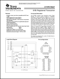
The FCT652T consists of bus transceiver circuits, D-type flip-flops, and control circuitry arranged for multiplexed transmission of data directly from the input bus or from the internal storage registers. GAB and GBA control pins are provided to control the transceiver functions. SAB and SBA control pins are provided to select either real-time or stored data transfer. The circuitry used for select control will eliminate the typical decoding glitch that occurs in a multiplexer during the transition between stored and real-time data. A LOW input level selects real-time data and a HIGH selects stored data. Data on the A or B data bus, or both, can be stored in the internal D flip-flops by LOW-to-HIGH transitions at the appropriate clock pins (CPAB or CPBA), regardless of the select or enable control pins. When SAB and SBA are in the real-time transfer mode, it is also possible to store data without using the internal D-type flip-flops by simultaneously enabling GAB and GBA. In this configuration, each output reinforces its input. Thus, when all other data sources to the two sets of bus lines are at high impedance, each set of bus lines will remain at its last state. |