|
|

|
|
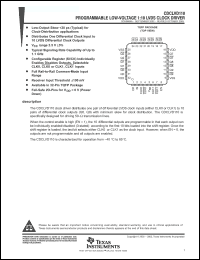
| Partname: | CDCLVD110VFG4 |
| Description: | 1-to-10 LVDS clock buffer up to 900MHz with minimum skew for clock distribution |
| Manufacturer: | Texas Instruments |
| Datasheet: | PDF (181K).
Click here to download *) |
The CDCLVD110 clock driver distributes one pair of differential LVDS clock inputs (either CLK0 or CLK1) to 10 pairs of differential clock outputs (Q0, Q9) with minimum skew for clock distribution. The CDCLVD110 is specifically designed for driving 50- transmission lines. When the control enable is high (EN = 1), the 10 differential outputs are programmable in that each output can be individually enabled/disabled (3-stated) according to the first 10 bits loaded into the shift register. Once the shift register is loaded, the last bit selects either CLK0 or CLK1 as the clock input. However, when EN = 0, the outputs are not programmable and all outputs are enabled. The CDCLVD110 is characterized for operation from -40C to 85C. |
|
Click here to download CDCLVD110VFG4 Datasheet*) |
 |
| *)Datasheets downloading from ChipDocs is only for our members (paid service). REGISTER NOW for your membership. |
|
|
|

