|
|

|
|
| Partname: | CDC9841DW |
| Description: | 3.3Vdriver |
| Manufacturer: | Texas Instruments |
| Datasheet: | PDF (136K).
Click here to download *) |
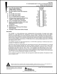
The CDC9841 generates all output frequencies from a 14.31818-MHz crystal input. A reference clock can be provided at X1 instead of a crystal input. Two phase-lock loops (PLLs) generate the CPU clock frequency and the 24-MHz clock frequency. On-chip loop filters and internal feedback eliminate the need for external components. The PCI and 12-MHz clock frequencies are derived from the base CPU and 24-MHz clock frequencies, respectively. The PLL circuit can be bypassed in the TEST mode (i.e., SEL0 = SEL1 = H) to distribute a test clock provided at the X1 input. Because the CDC9841 is based on PLL circuitry, it requires a stabilization time to achieve phase lock of the PLL. This stabilization time is required following power up and application of a fixed-frequency, fixed-phase signal at the X1 input, as well as following any changes to the SELn inputs. PCLKn and BCLKn provide low-skew/low-jitter clock signals for reliable clock operation. All outputs are 3 state and are enabled via OE. |
|

Click here to download CDC9841DW Datasheet*) |
 |
| *)Datasheets downloading from ChipDocs is only for our members (paid service). REGISTER NOW for your membership. |
|
|
|

