|
|

|
|
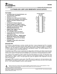
| Partname: | CDC536DBG4 |
| Description: | 3.3V PLL Clock Driver with 1/2x, 1x and 2x Frequency Options |
| Manufacturer: | Texas Instruments |
| Datasheet: | PDF (152K).
Click here to download *) |
The CDC536 is a high-performance, low-skew, low-jitter clock driver. It uses a phase-lock loop (PLL) to precisely align, in both frequency and phase, the clock output signals to the clock input (CLKIN) signal. It is specifically designed for use with synchronous DRAMs and popular microprocessors operating at speeds from 50 MHz to 100 MHz or down to 25 MHz on outputs configured as half-frequency outputs. The CDC536 operates at 3.3-V VCC and is designed to drive a 50-W transmission line. The feedback input (FBIN) is used to synchronize the output clocks in frequency and phase to the input clock (CLKIN). One of the six output clocks must be fed back to FBIN for the PLL to maintain synchronization between CLKIN and the outputs. The output used as the feedback pin is synchronized to the same frequency as CLKIN. The Y outputs can be configured to switch in phase and at the same frequency as CLKIN. The select (SEL) input configures three Y outputs to operate at one-half or double the CLKIN frequency depending on which pin is fed back to FBIN (see Tables 1 and 2). All output signal duty cycles are adjusted to 50% independent of the duty cycle at the input clock. |
|
Click here to download CDC536DBG4 Datasheet*) |
 |
| *)Datasheets downloading from ChipDocs is only for our members (paid service). REGISTER NOW for your membership. |
|
|
|

