|
|

|
|
| Partname: | CDC351IDW |
| Description: | 1-Line to 10-Line 3.3V Clock Driver with Tri-State Outputs |
| Manufacturer: | Texas Instruments |
| Datasheet: | PDF (215K).
Click here to download *) |
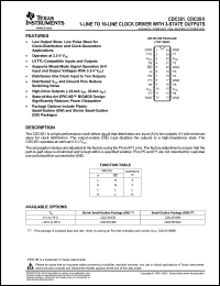
The CDC351 is a high-performance clock-driver circuit that distributes one input (A) to ten outputs (Y) with minimum skew for clock distribution. The output-enable (OE) input disables the outputs to a high-impedance state. The CDC351 operates at nominal 3.3-V VCC. The propagation delays are adjusted at the factory using the P0 and P1 pins. The factory adjustments ensure that the part-to-part skew is minimized and is kept within a specified window. Pins P0 and P1 are not intended for customer use and should be connected to GND. FUNCTION TABLE |
|
Click here to download CDC351IDW Datasheet*) |
 |
| *)Datasheets downloading from ChipDocs is only for our members (paid service). REGISTER NOW for your membership. |
|
|
|

