|
|

|
|
| Partname: | CDC2351DBG4 |
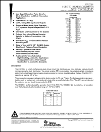
| Description: | 1-Line to 10-Line 3.3V Clock Driver with Tri-State Outputs |
| Manufacturer: | Texas Instruments |
| Datasheet: | PDF (222K).
Click here to download *) |
The CDC2351 is a high-performance clock-driver circuit that distributes one input (A) to ten outputs (Y) with minimum skew for clock distribution. The output-enable (OE) input disables the outputs to a high-impedance state. Each output has an internal series damping resistor to improve signal integrity at the load. The CDC2351 operates at nominal 3.3-V VCC. The propagation delays are adjusted at the factory using the P0 and P1 pins. The factory adjustments ensure that the part-to-part skew is minimized and is kept within a specified window. Pins P0 and P1 are not intended for customer use and should be connected to GND. The CDC2351 is characterized for operation from 0C to 70C. The CDC2351Q is characterized for operation over the full automotive temperature range of 40C to 125C. FUNCTION TABLE |
|
Click here to download CDC2351DBG4 Datasheet*) |
 |
| *)Datasheets downloading from ChipDocs is only for our members (paid service). REGISTER NOW for your membership. |
|
|
|

