|
|

|
|
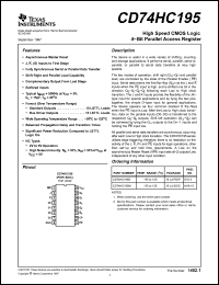
| Partname: | CD74HC195 |
| Description: | High Speed CMOS Logic 4-Bit Parallel Access Register |
| Manufacturer: | Texas Instruments |
| Datasheet: | PDF (42.2K).
Click here to download *) |
The two modes of operation, shift right (Q0-Q1) and parallel load, are controlled by the state of the Parallel Enable (PE) input. Serial data enters the first flip-flop (Q0) via the J and K inputs when the PE input is high, and is shifted one bit in the direction Q0-Q1-Q2-Q3 following each Low to High clock transition. The J and K inputs provide the flexibility of the JKtype input for special applications and by tying the two pins together, the simple D-type input for general applications. The device appears as four common-clocked D flip-flops when the PE input is Low. After the Low to High clock transition, data on the parallel inputs (D0-D3) is transferred to the respective Q0-Q3 outputs. Shift left operation (Q3-Q2) can be achieved by tying the Qn outputs to the Dn-1 inputs and holding the PE input low. |
|
Click here to download CD74HC195 Datasheet*) |
 |
| *)Datasheets downloading from ChipDocs is only for our members (paid service). REGISTER NOW for your membership. |
|
|
|

