|
|

|
|
| Partname: | CD74FCT654EN |
| Description: | FCT Interface Logic, Octal Bus Transceivers/ Registers, Open Drain (A Side), Three-State (B Side) |
| Manufacturer: | Texas Instruments |
| Datasheet: | PDF (49.1K).
Click here to download *) |
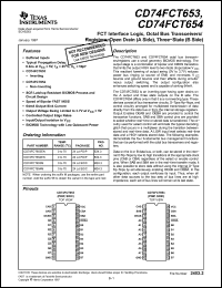
The CD74FCT653 and CD74FCT654 octal bus transceivers/registers use a small geometry BiCMOS technology. The output stage is a combination of bipolar and CMOS transistors that limits the output HIGH level to two diode drops below VCC. This resultant lowering of output swing (0V to 3.7V) reduces power bus ringing (a source of EMI) and minimizes VCC bounce and ground bounce and their effects during simultaneous output switching. The output configuration also enhances switching speed and is capable of sinking 64mA. The CD74FCT653 is an inverting type having open drains on the A output and three state outputs on the B side. The CD74FCT654 differs only in that it is a noninverting type. These devices consist of bus transceiver circuits, D-Type flip-flops, and control circuitry arranged for multiplexed transmission of data directly from the data bus or from the internal storage registers. Output Enables OEAB and OEBA are provided to control the transceiver functions. SAB and SBA control pins are provided to select whether real-time or stored data is transferred. The circuitry used for select control will eliminate the typical decoding glitch that occurs in a multiplexer during the transition between stored and real-time data. A LOW input level selects real-time data and a HIGH selects stored data. The following examples demonstrate the four fundamental bus management functions that can be performed with the octal bus transceivers and registers. Data on the A or B data bus, or both, can be stored in the internal D flip-flops by low to high transitions at the appropriate clock pins (CAB or CBA) regardless of the select or enable control pins. When SAB and SBA are in the real-time transfer mode, it is also possible to store data without using the internal D-Type flip-flops by simultaneously enabling OEAB and OEBA. In this configuration, each output reinforces its input. Thus, when all other data sources to the two sets of bus lines are at high impedance, each set of bus lines will remain at its last state. |
|

Click here to download CD74FCT654EN Datasheet*) |
 |
| *)Datasheets downloading from ChipDocs is only for our members (paid service). REGISTER NOW for your membership. |
|
|
|

