|
|

|
|
| Partname: | HD74LV2GT125AUSE |
| Description: | Dual Bus Buffer with 3-state Output / CMOS Logic Level Shifter |
| Manufacturer: | |
| Datasheet: | PDF (91.7K).
Click here to download *) |
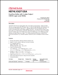
The HD74LV2GT125A has dual bus buffer with 3state output in an 8 pin package. Output is disabled when the associated output enable (OE) input is high. To ensure the high impedance state during power up or power down, OE should be connected to VCC through a pull-up resistor; the minimum value of the resistor is determined by the current sinking capability of the driver. The input protection circuitry on this device allows over voltage tolerance on the input, allowing the device to be used as a logiclevel translator from 3.0 V CMOS Logic to 5.0 V CMOS Logic or from 1.8 V CMOS logic to 3.0 V CMOS Logic while operating at the high-voltage power supply. Low voltage and high-speed operation is suitable for the battery powered products (e.g., notebook computers), and the low power consumption extends the battery life. |
|

Click here to download HD74LV2GT125AUSE Datasheet*) |
 |
| *)Datasheets downloading from ChipDocs is only for our members (paid service). REGISTER NOW for your membership. |
|
|
|

