ChipDocs - Datasheet Source for Semiconductor and Electronic Circuit Components
More than
480 535 
registered clients
Partname:PI74SSTVF16859
Description:13-Bit to 26-Bit Registered Buffer
Manufacturer:
Datasheet:PDF (193K).
Click here to download *)

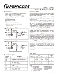
The device operates from a differential clock (CLK and CLK). Data registered at the crossing of CLK going HIGH, and CLK going LOW. The PI74SSTVF16859 supports low-power standby operation. When RESET is LOW, the differential input receivers are disabled, and undriven (floating) data, clock and reference voltage (VREF) inputs are allowed. In addition, when RESET is LOW, all registers are reset, and all outputs are forced LOW. The LVCMOS RESET input must always be held at a valid logic HIGH or LOW level.

Click here to download PI74SSTVF16859 Datasheet
*)
*)Datasheets downloading from ChipDocs is only for our members (paid service). REGISTER NOW for your membership.
Free Electronics Engineering Subscription
Win Win Circuit - PCB,PCBA,Touch Screen,LED Lighting
Win Win Circuit LTD. PCB, PCBA, LCD Module
www.wwteq.com
COPYRIGHT 1997-2024 ChipDocs  ALL RIGHT RESERVED