|
|

|
|
| Partname: | NBSG111BAR2 |
| Description: | 2.5 V/3.3 V SiGe 1:10 Differential Clock Driver with RSECL Outputs |
| Manufacturer: | ON Semiconductor |
| Datasheet: | PDF (87.0K).
Click here to download *) |
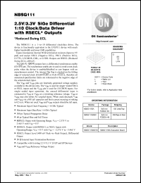
The Q[0:9] / Q[0:9] outputs have a differential synchronous enable (EN/EN) pin. The synchronous enable pin is used to avoid a runt clock pulse when the device is enabled/disabled as can happen with an asynchronous control. The internal flip flop is clocked on the falling edge of selected clock (CLK0/CLK0 or CLK1/CLK1), therefore all associated specification limits are referenced to the negative edge of the selected clock input. |
|

Click here to download NBSG111BAR2 Datasheet*) |
 |
| *)Datasheets downloading from ChipDocs is only for our members (paid service). REGISTER NOW for your membership. |
|
|
|

