|
|

|
|
| Partname: | NB3N502DR2G |
| Description: | PLL CLK MULTIPLIER |
| Manufacturer: | ON Semiconductor |
| Datasheet: | PDF (59.6K).
Click here to download *) |
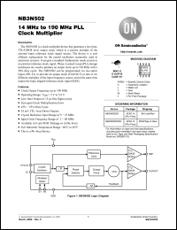
The NB3N502 is a clock multiplier device that generates a low jitter, TTL/CMOS level output clock which is a precise multiple of the external input reference clock signal source. The device is a cost efficient replacement for the crystal oscillators commonly used in electronic systems. It accepts a standard fundamental mode crystal or an external reference clock signal. Phase-Locked-Loop (PLL) design techniques are used to produce an output clock up to 190 MHz with a 50% duty cycle. The NB3N502 can be programmed via two select inputs (S0, S1) to provide an output clock (CLKOUT) at one of six different multiples of the input frequency source, and at the same time output the input aligned reference clock signal (REF). |
|
Click here to download NB3N502DR2G Datasheet*) |
 |
| *)Datasheets downloading from ChipDocs is only for our members (paid service). REGISTER NOW for your membership. |
|
|
|

