|
|

|
|
| Partname: | MC100E196FNR2G |
| Description: | BBG ECL PROG DELAY CHIP |
| Manufacturer: | ON Semiconductor |
| Datasheet: | PDF (180K).
Click here to download *) |
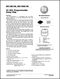
The delay section consists of a chain of gates and a linear ramp delay adjust organized as shown in the logic symbol. The first two delay elements feature gates that have been modified to have delays 1.25 and 1.5 times the basic gate delay of approximately 80 ps. These two elements provide the E196 with a digitally-selectable resolution of approximately 20 ps. The required device delay is selected by the seven address inputs D[0:6], which are latched on chip by a high signal on the latch enable (LEN) control. The FTUNE input takes an analog voltage and applies it to an internal linear ramp for reducing the 20 ps Least Significant Bit (LSB) minimum resolution still further. The FTUNE input is what differentiates the E196 from the E195. An eighth latched input, D7, is provided for cascading multiple PDC's for increased programmable range. The cascade logic allows full control of multiple PDC's, at the expense of only a single added line to the data bus for each additional PDC, without the need for any external gating. |
|

Click here to download MC100E196FNR2G Datasheet*) |
 |
| *)Datasheets downloading from ChipDocs is only for our members (paid service). REGISTER NOW for your membership. |
|
|
|

