|
|

|
|
| Partname: | M66851FP |
| Description: | SRAM type FIFO memory |
| Manufacturer: | Mitsubishi Electric Corp. |
| Package: | LQFP |
| Pins: | 32 |
| Oper. temp.: | -20 to 75 |
| Datasheet: | PDF (118K).
Click here to download *) |
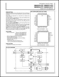
The write operation is controlled by a write clock pin(WCLK) and two write enable pins(WEN1,WEN2). Data present at the data input pins(D0-D8) is written into the Synchronous FIFO on every rising write clock edge when the device is enabled for writing. The read operation is controlled by a read clock pin(RCLK) and two read enable pins(REN1,REN2). Data is read from the Synchronous FIFO on every rising read clock edge when the device is enabled for reading. An output enable pin(OE) controls the states of the data output pins(Q0-Q8). MITSUBISHI FIFOs have four flags (EF,FF,PAE,PAF). The empty flag EF and the full flag FF are fixed flags. The almost empty flag PAE and the almost full flag PAF are programmable flags. The programmable flag offset is initiated by the load pin(LD). |
|
Click here to download M66851FP Datasheet*) |
 |
| *)Datasheets downloading from ChipDocs is only for our members (paid service). REGISTER NOW for your membership. |
|
|
|

