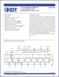
The QS5LV919 Clock Driver uses an internal phase locked loop (PLL) to lock low skew outputs to one of two reference clock inputs. Eight outputs are available: 2xQ, Q 0-Q 4, Q5, Q/2. Careful layout and design ensure < 300 ps skew between the Q 0-Q 4, and Q/2 outputs. The QS5LV919 includes an internal RC filter which provides excellent jitter characteristics and eliminates the need for external components. Various combinations of feedback and a divide-by-2 in the VCO path allow applications to be customized for linear VCO operation over a wide range of input SYNC frequencies. The PLL can also be disabled by the PLL_EN signal to allow low frequency or DC testing. The LOCK output asserts to indicate when phase lock has been achieved. The QS5LV919 is designed for use in high-performance workstations, multiboard computers, networking hardware, and mainframe systems. Several can be used in parallel or scattered throughout a system for guaranteed low skew, system-wide clock distribution networks. For more information on PLL clock driver products, see Application Note AN-227. |