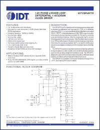
The CSPU877D is a PLL based clock driver that acts as a zero delay buffer to distribute one differential clock input pair(CLK, CLK ) to 10 differential output pairs (Y [0:9], Y [0:9]) and one differential pair of feedback clock output (FBOUT, FBOUT). External feedback pins (FBIN, FBIN) for synchronization of the outputs to the input reference is provided. OE, OS, and AVDD control the power-down and test mode logic. When AVDD is grounded, the PLL is turned off and bypassed for test mode purposes. When the differential clock inputs (CLK, CLK) are both at logic low, this device will enter a low power-down mode. In this mode, the receivers are disabled, the PLL is turned off, and the output clock drivers are disabled, resulting in a current consumption device of less than 500A. |