|
|

|
|
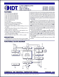
| Partname: | IDT72V201L15J |
| Description: | 3.3 VOLT CMOS SyncFIFO?? 256 x 9, 512 x 9, 1,024 x 9, 2,048 x 9, 4,096 x 9 and 8,192 x 9 |
| Manufacturer: | Integrated Device Technology |
| Datasheet: | PDF (115K).
Click here to download *) |
These FIFOs have 9-bit input and output ports. The input port is controlled by a free-running clock (WCLK), and two Write Enable pins (WEN1, WEN2). Data is written into the Synchronous FIFO on every rising clock edge when the Write Enable pins are asserted. The output port is controlled by another clock pin (RCLK) and two Read Enable pins ( REN1, REN2). The Read Clock can be tied to the Write Clock for single clock operation or the two clocks can run asynchronous of one another for dualclock operation. An Output Enable pin (OE) is provided on the read port for three-state control of the output. The Synchronous FIFOs have two fixed flags, Empty (EF) and Full (FF). Two programmable flags, Almost-Empty (PAE) and Almost-Full (PAF), are provided for improved system control. The programmable flags default to Empty+7 and Full-7 for PAE and PAF, respectively. The programmable flag offset loading is controlled by a simple state machine and is initiated by asserting the Load pin (LD). |
|
Click here to download IDT72V201L15J Datasheet*) |
 |
| *)Datasheets downloading from ChipDocs is only for our members (paid service). REGISTER NOW for your membership. |
|
|
|

