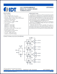
The IDT5V991A is a high fanout 3.3V PLL based clock driver intended for high performance computing and data-communications applications. A key feature of the programmable skew is the ability of outputs to lead or lag the REF input signal. The IDT5V991A has eight programmable skew outputs in four banks of 2. Skew is controlled by 3-level input signals that may be hard-wired to appropriate HIGH-MID-LOW levels. When the GND/sOE pin is held low, all the outputs are synchronously enabled. However, if GND/sOE is held high, all the outputs except 3Q0 and 3Q1 are synchronously disabled. Furthermore, when the VCCQ/PE is held high, all the outputs are synchronized with the positive edge of the REF clock input. When VCCQ/ PE is held low, all the outputs are synchronized with the negative edge of REF. Both devices have LVTTL outputs with 12mA balanced drive outputs. |