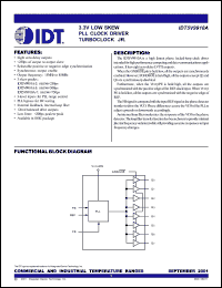
The IDT5V9910A is a high fanout phase locked-loop clock driver intended for high performance computing and data-communications applications. It has eight zero delay LVTTL outputs. When the GND/sOE pin is held low, all the outputs are synchronously enabled. However, if GND/sOE is held high, all the outputs except Q2 and Q3 are synchronously disabled. Furthermore, when the VCCQ/PE is held high, all the outputs are synchronized with the positive edge of the REF clock input. When V CCQ/ PE is held low, all the outputs are synchronized with the negative edge of REF. |