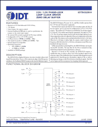
The IDT5V2528 inputs, PLL core, Y0, Y1, and FBOUT buffers operate from the 3.3V VDD and AVDD power supply pins. One bank of ten outputs provide low-skew, low-jitter copies of CLK. Of the ten outputs, up to seven may be configured for 2.5V or 3.3V LVTTL outputs. The number of 2.5V outputs is controlled by 3-level input signals G_Ctrl and T_Ctrl, and by connecting the appropriate VDDQ pins to 2.5V or 3.3V. The 3-level input signals may be hard-wired to high-mid-low levels. Output signal duty cycles are adjusted to 50 percent, independent of the duty cycle at CLK. The outputs can be enabled or disabled via the G_Ctrl input. When the G_Ctrl input is mid or high, the outputs switch in phase and frequency with CLK; when the G_Ctrl is low, all outputs (except FBOUT) are disabled to the logic-low state. Unlike many products containing PLLs, the IDT5V2528 does not require external RC networks. The loop filter for the PLL is included on-chip, minimizing component count, board space, and cost. Because it is based on PLL circuitry, the IDT5V2528 requires a stabilization time to achieve phase lock of the feedback signal to the reference signal. This stabilization time is required, following power up and application of a fixed-frequency, fixed-phase signal at CLK, as well as following any changes to the PLL reference or feedback signals. The PLL can be bypassed for test purposes by strapping AVDD to ground. |