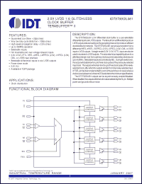
The IDT5T93GL061 2.5V differential clock buffer is a user-selectable differential input to six LVDS outputs . The fanout from a differential input to six LVDS outputs reduces loading on the preceding driver and provides an efficient clock distribution network. The IDT5T93GL061 can act as a translator from a differential HSTL, eHSTL, LVEPECL (2.5V), LVPECL (3.3V), CML, or LVDS input to LVDS outputs. A single-ended 3.3V / 2.5V LVTTL input can also be used to translate to LVDS outputs. The redundant input capability allows for a glitchless change-over from a primary clock source to a secondary clock source up to 450MHz. Selectable inputs are controlled by SEL. During the switchover, the output will disable low for up to three clock cycles of the previously-selected input clock. The outputs will remain low for up to three clock cycles of the newlyselected clock, after which the outputs will start from the newly-selected input. A FSEL pin has been implemented to control the switchover in cases where a clock source is absent or is driven to DC levels below the minimum specifications. The IDT5T93GL061 outputs can be asynchronously enabled/disabled. When disabled, the outputs will drive to the value selected by the GL pin. Multiple power and grounds reduce noise. |