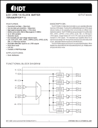
The IDT5T9306 2.5V differential clock buffer is a user-selectable differential input to six LVDS outputs. The fanout from a differential input to six LVDS outputs reduces loading on the preceding driver and provides an efficient clock distribution network. The IDT5T9306 can act as a translator from a differential HSTL, eHSTL, LVEPECL (2.5V), LVPECL (3.3V), CML, or LVDS input to LVDS outputs. A single-ended 3.3V / 2.5V LVTTL input can also be used to translate to LVDS outputs. The redundant input capability allows for an asynchronous change-over from a primary clock source to a secondary clock source. Selectable reference inputs are controlled by SEL. The IDT5T9306 outputs can be asynchronously enabled/disabled. When disabled, the outputs will drive to the value selected by the GL pin. Multiple power and grounds reduce noise. |