|
|

|
|
| Partname: | ICS873991AY-147LF |
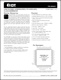
| Description: | LOW VOLTAGE, LVCMOS/LVPECL-TO LVPECL/ECL CLOCK GENERATOR |
| Manufacturer: | Integrated Device Technology |
| Datasheet: | PDF (414K).
Click here to download *) |
The four independent banks of outputs each have their own output dividers, which allow the device to generate a multitude of different bank frequency ratios and output-to-input frequency ratios. The output frequency range is 25MHz to 500MHz and the input frequency range is 6.25MHz to 125MHz. The PLL_SEL input can be used to bypass the PLL for test and system debug purposes. In bypass mode, the input clock is routed around the PLL and into the internal output dividers. |
|
Click here to download ICS873991AY-147LF Datasheet*) |
 |
| *)Datasheets downloading from ChipDocs is only for our members (paid service). REGISTER NOW for your membership. |
|
|
|

