|
|

|
|
| Partname: | ICS9214YGLF-T |
| Description: | Rambus XDR Clock Generator |
| Manufacturer: | |
| Datasheet: | PDF (216K).
Click here to download *) |
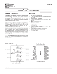
The PLL receives a reference clock, CLK_INT/C and outputs a clock signal at a frequency equal to the input frequency times a multiplier. Table 2 shows the multipliers selectable via the SMBus interface. This clock signal is then fed to the differential output buffers to drive the enabled clocks. Disabled outputs are set to Hi-Z. The Bypass mode routes the input clock, CLK_INT/C, directly to the differential output buffers, bypassing the PLL. |
|
Click here to download ICS9214YGLF-T Datasheet*) |
 |
| *)Datasheets downloading from ChipDocs is only for our members (paid service). REGISTER NOW for your membership. |
|
|
|

