|
|

|
|
| Partname: | ICS8344BYI-T |
| Description: | Low skew 1 to 24 differential to LVCMOS fanout buffer |
| Manufacturer: | |
| Package: | LQFP |
| Pins: | 48 |
| Oper. temp.: | -40 to 85 |
| Datasheet: | PDF (142K).
Click here to download *) |
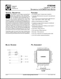
The ICS8344I is a low voltage, low skew fanout buffer and a member of the H iPerClockSTM HiPerClockSTM family of High Performance Clock Solutions from ICS. The ICS8344I has two selectable clock inputs. The CLK0, nCLK0 and CLK1, nCLK1 pairs can accept most standard differential input levels. The ICS8344I is designed to translate any differential signal levels to LVCMOS levels. The low impedance LVCMOS outputs are designed to drive 50 series or parallel terminated transmission lines. The effective fanout can be increased to 48 by utilizing the ability of the outputs to drive two series terminated lines. Redundant clock applications can make use of the dual clock input. The dual clock inputs also facilitate board level testing. ICS8344I is characterized at full 3.3V, full 2.5V and mixed 3.3V input and 2.5V output operating supply modes. |
|
Click here to download ICS8344BYI-T Datasheet*) |
 |
| *)Datasheets downloading from ChipDocs is only for our members (paid service). REGISTER NOW for your membership. |
|
|
|

