|
|

|
|
| Partname: | GS840H18AB-166 |
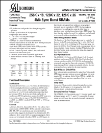
| Description: | 166MHz 8.5ns 256K x 18 4Mb sync burst SRAM |
| Manufacturer: | |
| Package: | BGA |
| Pins: | 119 |
| Oper. temp.: | 0 to 70 |
| Datasheet: | PDF (910K).
Click here to download *) |
The function of the Data Output register can be controlled by the user via the FT mode pin/bump (Pin 14 in the TQFP and Bump 5R in the BGA, ). Holding the FT mode pin/bump low places the RAM in Flow Through mode, causing output data to bypass the Data Output Register. Holding FT high places the RAM in Pipeline mode, activating the rising-dge-triggered Data Output Register. |
|

Click here to download GS840H18AB-166 Datasheet*) |
 |
| *)Datasheets downloading from ChipDocs is only for our members (paid service). REGISTER NOW for your membership. |
|
|
|

