|
|

|
|
| Partname: | GS820H32T-5I |
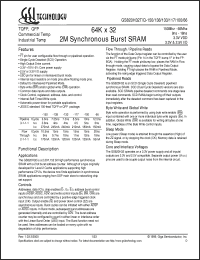
| Description: | 100MHz 12ns 64K x 32 2M synchronous burst SRAM |
| Manufacturer: | |
| Package: | TQFP |
| Pins: | 100 |
| Oper. temp.: | -40 to 85 |
| Datasheet: | PDF (342K).
Click here to download *) |
The function of the Data Output register can be controlled by the user via the FT mode pin/bump (Pin 14 in the TQFP, bump 1F in the FPBGA). Holding the FT mode pin/bump low, places the RAM in Flow through mode, causing output data to bypass the Data Output Register. Holding FT high places the RAM in Pipelined Mode, activating the rising edge triggered Data Output Register. |
|

Click here to download GS820H32T-5I Datasheet*) |
 |
| *)Datasheets downloading from ChipDocs is only for our members (paid service). REGISTER NOW for your membership. |
|
|
|

