|
|

|
|
| Partname: | XRK39351_0611 |
| Description: | 3.3V OR 2.5V, 9-OUTPUT PLL CLOCK DRIVER |
| Manufacturer: | Exar |
| Datasheet: | PDF (293K).
Click here to download *) |
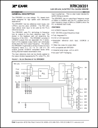
The XRK39351 uses PLL technology to frequency lock its outputs to the clock reference input. The divider in the feedback path will determine the frequency of the VCO. The XRK39351 provides 9 LVCMOS outputs that are separated into 4 banks. Each of the separate output banks can individually divide down the VCO output frequency. This allows the XRK39351 to generate a variety of output-to-input frequency ratios (1:1, 1:2, 1:4, 2:1 and 4:1). All outputs provide LVCMOS compatible levels while driving 50 terminated transmission lines. The input reference clock can be directly applied to the output dividers bypassing the PLL when PLL_EN |
|
Click here to download XRK39351_0611 Datasheet*) |
 |
| *)Datasheets downloading from ChipDocs is only for our members (paid service). REGISTER NOW for your membership. |
|
|
|

