|
|

|
|
| Partname: | EVDD415 |
| Description: | Gate driver IC evaluation board |
| Manufacturer: | |
| Package: | -- |
| Datasheet: | PDF (134K).
Click here to download *) |
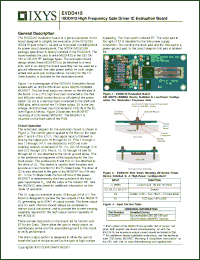
The EVDD415 evaluation board is a general-purpose circuit board designed to simplify the evaluation of the IXYS/DEI IXDD415 gate drive IC, as well as to provide a building block for power circuit development. The IXDD415SI SO-28 package gate driver is factory-installed in the EVDD415. The board enables the user to drive MOSFETs in the DEI DE150 or DE-275 RF package types. The evaluation board design allows these MOSFETS to be attached to a heat sink, and in so doing the board assembly can be used as a ground referenced, low side power switch for both singleended and push-pull configurations. Circuitry for the TriState function is included on the evaluation board. Figure 1 is a photograph of the IXDD415 Evaluation Board loaded with an IXDD415SI driver and a DE275-102N06A MOSFET. The low level inputs are shown on the left side of the board. J1 is a TTL high true input connected to the INA and INB pins which control the on or off state of the power switch U2. E9 is a low true input connected to the ENA and ENB pins, which control the Tri-State output. E1 is the low voltage, (8-30V) power input connected to VCC-IN of the IC, (see Figure 3 below). Figure 2 illustrates the MOSFET mounting of a DE-Series MOSFET. The MOSFET is mounted on the back side of the PCB. Circuit Operation |
|
Click here to download EVDD415 Datasheet*) |
 |
| *)Datasheets downloading from ChipDocs is only for our members (paid service). REGISTER NOW for your membership. |
|
|
|

