|
|

|
|
| Partname: | CY7C4291V-15JI |
| Description: | 128K x 9 low voltage Deep Sync FIFO, 15ns |
| Manufacturer: | Cypress Semiconductor |
| Package: | PLCC |
| Pins: | 32 |
| Oper. temp.: | -40 to 85 |
| Datasheet: | PDF (234K).
Click here to download *) |
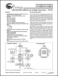
These FIFOs have 9-bit input and output ports that are controlled by separate clock and enable signals. The input port is controlled by a free-running clock (WCLK) and two writeenable pins (WEN1, WEN2/LD). When WEN1 is LOW and WEN2/LD is HIGH, data is written into the FIFO on the rising edge of the WCLK signal. While WEN1 and WEN2/LD are held active, data is continually written into the FIFO on each WCLK cycle. The output port is controlled in a similar manner by a free-running read clock (RCLK) and two read enable pins (REN1, REN2). In addition, the CY7C4261/71/81/91V has an output enable pin (OE). The read (RCLK) and write (WCLK) clocks may be tied together for single-clock operation or the two clocks may be run independently for asynchronous read/write applications. Clock frequencies up to 100 MHz are achievable. Depth expansion is possible using one enable input for system control, while the other enable is controlled by expansion logic to direct the flow of data. |
|

Click here to download CY7C4291V-15JI Datasheet*) |
 |
| *)Datasheets downloading from ChipDocs is only for our members (paid service). REGISTER NOW for your membership. |
|
|
|

