|
|

|
|
| Partname: | CY7C4255-10ACT |
| Description: | 8K X 18 SYNCHRONOUS FIFO |
| Manufacturer: | Cypress Semiconductor |
| Datasheet: | PDF (350K).
Click here to download *) |
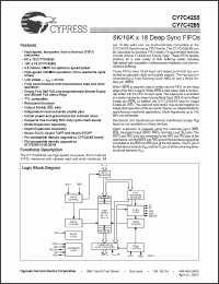
These FIFOs have 18-bit input and output ports that are controlled by separate clock and enable signals. The input port is controlled by a Free-Running Clock (WCLK) and a Write Enable pin (WEN). When WEN is asserted, data is written into the FIFO on the rising edge of the WCLK signal. While WEN is held active, data is continually written into the FIFO on each cycle. The output port is controlled in a similar manner by a free-running Read Clock (RCLK) and a Read Enable pin (REN). In addition, the CY7C4255/65 have an Output Enable pin (OE). The read and write clocks may be tied together for single-clock operation or the two clocks may be run independently for asynchronous read/write applications. Clock frequencies up to 100 MHz are achievable. |
|

Click here to download CY7C4255-10ACT Datasheet*) |
 |
| *)Datasheets downloading from ChipDocs is only for our members (paid service). REGISTER NOW for your membership. |
|
|
|

