|
|

|
|
| Partname: | CY7C401 |
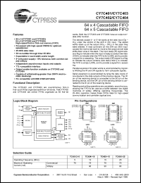
| Description: | 64 x 4 Cascadable FIFO / 64 x 5 Cascadable FIFO |
| Manufacturer: | Cypress Semiconductor |
| Datasheet: | PDF (270K).
Click here to download *) |
The devices accept 4- or 5-bit words at the data input (DI0 DIn) under the control of the shift in (SI) input. The stored words stack up at the output (DO0 DOn) in the order they were entered. A read command on the shift out (SO) input causes the next to last word to move to the output and all data shifts down once in the stack. The input ready (IR) signal acts as a flag to indicate when the input is ready to accept new data (HIGH), to indicate when the FIFO is full (LOW), and to provide a signal for a cascading. The output ready (OR) signal is a flag to indicate the output contains valid data (HIGH), to indicate the FIFO is empty (LOW), and to provide a signal for cascading. Parallel expansion for wider words is accomplished by logically ANDing the IR and OR signals to form composite signals. Serial expansion is accomplished by tying the data inputs of one device to the data outputs of the previous device. The IR pin of the receiving device is connected to the SO pin of the sending device, and the OR pin of the sending device is connected to the SI pin of the receiving device. |
|

Click here to download CY7C401 Datasheet*) |
 |
| *)Datasheets downloading from ChipDocs is only for our members (paid service). REGISTER NOW for your membership. |
|
|
|

