|
|

|
|
| Partname: | CY7C1373B-83BGI |
| Description: | 512K x 36/1M x 18 Flow-Thru SRAM with NoBL Architecture |
| Manufacturer: | Cypress Semiconductor |
| Datasheet: | PDF (876K).
Click here to download *) |
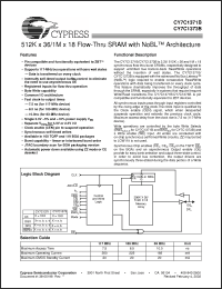
The CY7C1371B/CY7C1373B is 3.3V, 512K x 36 and 1M x 18 synchronous flow-thru burst SRAMs, respectively designed to support unlimited true back-to-back Read/Write operations without the insertion of wait states. The CY7C1371B/ CY7C1373B is equipped with the advanced No Bus LatencyTM (NoBL) logic required to enable consecutive Read/Write operations with data being transferred on every clock cycle. This feature dramatically improves the throughput of data through the SRAM, especially in systems that require frequent Write/Read transitions.The CY7C1371B/CY7C1373B is pin compatible and functionally equivalent to ZBT devices. All synchronous inputs pass through input registers controlled by the rising edge of the clock.The clock input is qualified by the Clock enable (CEN) signal, which when deasserted suspends operation and extends the previous clock cycle. Maximum access delay from the clock rise is 7.5 ns (117-MHz device). |
|

Click here to download CY7C1373B-83BGI Datasheet*) |
 |
| *)Datasheets downloading from ChipDocs is only for our members (paid service). REGISTER NOW for your membership. |
|
|
|

