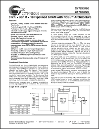
The CY7C1370B and CY7C1372B SRAMs are designed to eliminate dead cycles when transitions from Read to Write or vice versa. These SRAMs are optimized for 100 percent bus utilization and achieve Zero Bus Latency. They integrate 524,288 x 36 and 1,048,576 x 18 SRAM cells, respectively, with advanced synchronous peripheral circuitry and a 2-bit counter for internal burst operation. The Synchronous Burst SRAM family employs high-speed, low-power CMOS designs using advanced single-layer polysilicon, three-layer metal technology. Each memory cell consists of six transistors. All synchronous inputs are gated by registers controlled by a positive-edge-triggered Clock input (CLK). The synchronous |