|
|

|
|
| Partname: | CY7C1325-117AC |
| Description: | 256K x 18 Synchronous 3.3V Cache RAM |
| Manufacturer: | Cypress Semiconductor |
| Datasheet: | PDF (268K).
Click here to download *) |
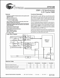
The CY7C1325 allows both an interleaved or linear burst sequences, selected by the MODE input pin. A HIGH selects an interleaved burst sequence, while a LOW selects a linear burst sequence. Burst accesses can be initiated with the Processor Address Strobe (ADSP) or the Cache Controller Address Strobe (ADSC) inputs. Address advancement is controlled by the Address Advancement (ADV) input. A synchronous self-timed write mechanism is provided to simplify the write interface. A synchronous chip enable input and an asynchronous output enable input provide easy control for bank selection and output three-state control. |
|
Click here to download CY7C1325-117AC Datasheet*) |
 |
| *)Datasheets downloading from ChipDocs is only for our members (paid service). REGISTER NOW for your membership. |
|
|
|

