|
|

|
|
| Partname: | CY7C1302CV25-167 |
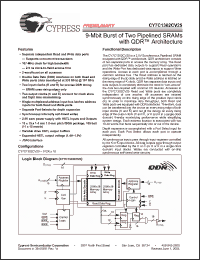
| Description: | 9-Mbit Burst of Two Pipelined SRAMs with QDR??? Architecture |
| Manufacturer: | Cypress Semiconductor |
| Datasheet: | PDF (296K).
Click here to download *) |
The CY7C1302CV25 is a 2.5V Synchronous Pipelined SRAM equipped with QDRTM architecture. QDR architecture consists of two separate ports to access the memory array. The Read port has dedicated data outputs to support Read operations and the Write Port has dedicated data inputs to support Write operations. Access to each port is accomplished through a common address bus. The Read address is latched on the rising edge of the K clock and the Write address is latched on the rising edge of K clock. QDR has separate data inputs and data outputs to completely eliminate the need to "turn-around" the data bus required with common I/O devices. Accesses to the CY7C1302CV25 Read and Write ports are completely independent of one another. All accesses are initiated synchronously on the rising edge of the positive input clock (K). In order to maximize data throughput, both Read and Write ports are equipped with DDR interfaces. Therefore, data can be transferred into the device on every rising edge of both input clocks (K and K) and out of the device on every rising edge of the output clock (C and C, or K and K in a single clock domain) thereby maximizing performance while simplifying system design. Each address location is associated with two 18-bit words that burst sequentially into or out of the device. Depth expansion is accomplished with a Port Select input for each port. Each Port Select allows each port to operate independently. |
|
Click here to download CY7C1302CV25-167 Datasheet*) |
 |
| *)Datasheets downloading from ChipDocs is only for our members (paid service). REGISTER NOW for your membership. |
|
|
|

