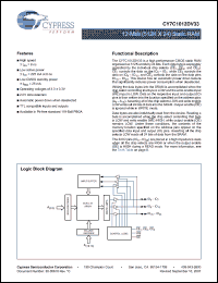
The CY7C1012DV33 is a high performance CMOS static RAM organized as 512K words by 24 bits. Each data byte is separately controlled by the individual chip selects (CE1, CE2, and CE3). CE1 controls the data on the IO0 IO7, while CE2 controls the data on IO8 IO15, and CE3 controls the data on the data pins IO16 IO23. This device has an automatic power down feature that significantly reduces power consumption when deselected. Writing the data bytes into the SRAM is accomplished when the chip select controlling that byte is LOW and the write enable input (WE) input is LOW. Data on the respective input and output (IO) pins is then written into the location specified on the address pins (A0 A18). Asserting all of the chip selects LOW and write enable LOW writes all 24 bits of data into the SRAM. Output enable (OE) is ignored while in WRITE mode. Data bytes are also individually read from the device. Reading a byte is accomplished when the chip select controlling that byte is LOW and write enable (WE) HIGH, while output enable (OE) remains LOW. Under these conditions, the contents of the memory location specified on the address pins appear on the specified data input and output (IO) pins. Asserting all the chip selects LOW reads all 24 bits of data from the SRAM. The 24 IO pins (IO0 IO23) are placed in a high impedance state when all the chip selects are HIGH or when the output enable (OE) is HIGH during a READ mode. For more information, see the Truth Table on page 8. |