|
|

|
|
| Partname: | CY2V9950AI |
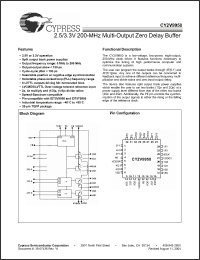
| Description: | 2.5/3.3V 200-MHz Multi-Output Zero Delay Buffer |
| Manufacturer: | Cypress Semiconductor |
| Datasheet: | PDF (251K).
Click here to download *) |
The user can program the output banks through 3F[0:1] and 4F[0:1]pins. Any one of the outputs can be connected to feedback input to achieve different reference frequency multiplication and divide ratios and zero input-output delay. The device also features split output bank power supplies which enable the user to run two banks (1Qn and 2Qn) at a power supply level different from that of the other two banks (3Qn and 4Qn). Additionally, the PE pin controls the synchronization of the output signals to either the rising or the falling edge of the reference clock. |
|
Click here to download CY2V9950AI Datasheet*) |
 |
| *)Datasheets downloading from ChipDocs is only for our members (paid service). REGISTER NOW for your membership. |
|
|
|

