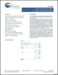
The CY29352 features an LVCMOS reference clock input and provides 11 outputs partitioned in three banks of five, four, and two outputs. Bank A divides the VCO output by four and six while bank B divides by four and two, and bank C divides by two and four per SEL(A:C) settings, see Table 3 on page 3. These dividers allow output to input ratios of 3:1, 2:1, 3:2, 1:1, 2:3, 1:2, and 1:3. Each LVCMOS compatible output drives 50 series or parallel terminated transmission lines. For series terminated transmission lines, each output drives one or two traces, giving the device an effective fanout of 1:22. The PLL is stable if the VCO is configured to run between 200 MHz to 500 MHz. This allows a wide range of output frequencies from 16.67 MHz to 200 MHz. For normal operation, the external feedback input, FB_IN, is connected to one of the outputs. The internal VCO runs at multiples of the input reference clock set by the feedback divider, see Table 2 on page 3. When PLL_EN# is HIGH, PLL is bypassed and the reference clock directly feeds the output dividers. This mode is fully static and the minimum input clock frequency specification does not apply. |