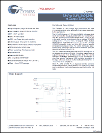
The CY29351 features LVPECL and LVCMOS reference clock inputs and provides 9 outputs partitioned in four banks of one, one, two, and five outputs. Bank A divides the VCO output by two or four while the other banks divide by four or eight per SEL(A:D) settings (Table 3, "Function Table," on page 3). These dividers allow output to input ratios of 4:1, 2:1, 1:1, 1:2, and 1:4. Each LVCMOS compatible output can drive 50 series or parallel terminated transmission lines. For series terminated transmission lines, each output can drive one or two traces giving the device an effective fanout of 1:18. The PLL is ensured stable given that the VCO is configured to run between 200 MHz to 500 MHz. This allows a wide range of output frequencies from 25 MHz to 200 MHz. For normal operation, the external feedback input, FB_IN, is connected to one of the outputs. The internal VCO is running at multiples of the input reference clock set by the feedback divider (Table 2, "Frequency Table," on page 3). When PLL_EN# is LOW, PLL is bypassed and the reference clock directly feeds the output dividers. This mode is fully static and the minimum input clock frequency specification does not apply. |