ChipDocs - Datasheet Source for Semiconductor and Electronic Circuit Components
More than
12 598 333 
queries processed
Partname:CY29351AI
Description:2.5V or 3.3V, 200-MHz, 9-Output Zero Delay Buffer
Manufacturer:Cypress Semiconductor
Datasheet:PDF (286K).
Click here to download *)

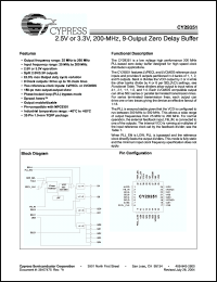
The CY29351 features LVPECL and LVCMOS reference clock inputs and provides 9 outputs partitioned in 4 banks of 1, 1, 2, and 5 outputs. Bank A divides the VCO output by 2 or 4 while the other banks divide by 4 or 8 per SEL(A:D) settings, see Functional Table. These dividers allow output to input ratios of 4:1, 2:1, 1:1, 1:2, and 1:4. Each LVCMOS compatible output can drive 50 series or parallel terminated transmission lines. For series terminated transmission lines, each output can drive one or two traces giving the device an effective fanout of 1:18.

Click here to download CY29351AI Datasheet
*)
*)Datasheets downloading from ChipDocs is only for our members (paid service). REGISTER NOW for your membership.
Free Electronics Engineering Subscription
Win Win Circuit - PCB,PCBA,Touch Screen,LED Lighting
Win Win Circuit LTD. PCB, PCBA, LCD Module
www.wwteq.com
COPYRIGHT 1997-2024 ChipDocs  ALL RIGHT RESERVED