|
|

|
|
| Partname: | CY2308SC-3T |
| Description: | 3.3V Zero Delay Buffer |
| Manufacturer: | Cypress Semiconductor |
| Datasheet: | PDF (377K).
Click here to download *) |
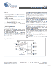
The CY2308 has two banks of four outputs each that is controlled by the select inputs as shown in the table Select Input Decoding on page 2. If all output clocks are not required, Bank B is three-stated. The input clock is directly applied to the output for chip and system testing purposes by the select inputs. The CY2308 PLL enters a power down state when there are no rising edges on the REF input. In this mode, all outputs are three-stated and the PLL is turned off resulting in less than 50 A of current draw. The PLL shuts down in two additional cases as shown in the table Select Input Decoding on page 2. Multiple CY2308 devices accept the same input clock and distribute it in a system. In this case, the skew between the outputs of two devices is less than 700 ps. |
|
Click here to download CY2308SC-3T Datasheet*) |
 |
| *)Datasheets downloading from ChipDocs is only for our members (paid service). REGISTER NOW for your membership. |
|
|
|

