|
|

|
|
| Partname: | AZ100LVE210FNR2 |
| Description: | 3.0 V-5.5 V, ECL/PECL 1:4, 1:5 differential clock driver |
| Manufacturer: | |
| Package: | PLCC |
| Pins: | 28 |
| Oper. temp.: | -40 to 85 |
| Datasheet: | PDF (143K).
Click here to download *) |
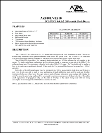
The AZ100LVE210 is a low skew 1:4, 1:5 fanout buffer designed with clock distribution in mind. The device features fully differential clock paths to minimize both device and system skew. The AZ100LVE210 offers two selectable clock inputs allowing redundant or test clocks to be incorporated into the system clock trees. The AZ100LVE210 provides a VBB output for single-ended use or a DC bias reference for AC coupling to the device. For singleended input applications, the VBB reference should be connected to one side of the CLKa/CLKb differential input pair. The input signal is then fed to the other CLKa/CLKb input. The VBB should only be used as a bias for its sink/source capability is limited. When used, the VBB pin should be bypassed to ground via a 0.01F capacitor. |
|

Click here to download AZ100LVE210FNR2 Datasheet*) |
 |
| *)Datasheets downloading from ChipDocs is only for our members (paid service). REGISTER NOW for your membership. |
|
|
|

