|
|

|
|
| Partname: | AS5C4009LLCW-85/883C |
| Description: | 512K x 8 SRAM - ultra low power |
| Manufacturer: | |
| Package: | DIP |
| Pins: | 32 |
| Oper. temp.: | -55 to 125 |
| Datasheet: | PDF (148K).
Click here to download *) |
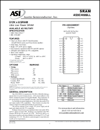
The AS5C4009LL is organized as 524,288 x 8 SRAM utilizing a special ultra low power design process. ASI's pinout adheres to the JEDEC standard for pinout on 4 megabit SRAMs. The evolutionary 32 pin version allows for easy upgrades from the 1 meg SRAM design. For flexibility in memory applications, ASI offers chip enable (CE) and output enable (OE) capabilities. These features can place the outputs in High-Z for additional flexibility in system design. This devices operates from a single +5V power supply and all inputs and outputs are fully TTL-compatible. Writing to these devices is accomplished when write enable (WE) and CE inputs are both LOW. Reading is accomplished when WE remains HIGH and CE and OE go LOW. The device offers a reduced power standby mode when disabled, by lowering VCC to 2V and maintaining CE = 2V. This allows system designers to meet ultra low standby power requirements. |
|
Click here to download AS5C4009LLCW-85/883C Datasheet*) |
 |
| *)Datasheets downloading from ChipDocs is only for our members (paid service). REGISTER NOW for your membership. |
|
|
|

