|
|

|
|
| Partname: | LCK4993KB-DB |
| Description: | Low-Voltage PLL Clock Drivers |
| Manufacturer: | Agere Systems |
| Datasheet: | PDF (352K).
Click here to download *) |
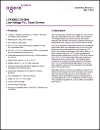
The LCK4993 and LCK4994 low-voltage PLL clock drivers offer user-selectable control over system clock functions. The multiple-output clock drivers provide the system integrator with functions necessary to optimize the timing of high-performance computer and communication systems. Each of the eighteen configurable outputs drive terminated transmission lines with impedances as low as 50 while delivering minimal and specified output skews at LVTTL levels. The outputs are arranged in five banks. Banks 1--4 allow a divide function of 1 to 12, while simultaneously allowing phase adjustments in 625 ps--1300 ps increments up to 10.4 ns. One of the output banks also includes an independent clock invert function. The feedback bank consists of two outputs that allow divide-by functionality from 1 to 12 and limited phase adjustments. Any one of these eighteen outputs can be connected to the feedback input or drive other inputs. |
|

Click here to download LCK4993KB-DB Datasheet*) |
 |
| *)Datasheets downloading from ChipDocs is only for our members (paid service). REGISTER NOW for your membership. |
|
|
|

