|
|

|
|
| Partname: | AD8402AR50 |
| Description: | 0.3-8V; 1/2/4-channel digital potentiometers. For mechanical potentiometer replacement, programmable filters, delays, time constants, volume control, panning, line impendance matching, power supply adjustment |
| Manufacturer: | Analog Devices |
| Package: | SOIC |
| Pins: | 14 |
| Oper. temp.: | -40 to 125 |
| Datasheet: | PDF (443K).
Click here to download *) |
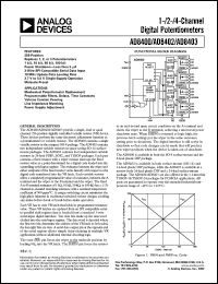
The AD8400/AD8402/AD8403 provide a single, dual or quad channel, 256 position digitally controlled variable resistor (VR) device. These devices perform the same electronic adjustment function as a potentiometer or variable resistor. The AD8400 contains a single variable resistor in the compact SO-8 package. The AD8402 contains two independent variable resistors in space-saving SO-14 surfacemount packages. The AD8403 contains four independent variable resistors in 24-lead PDIP, SOIC, and TSSOP packages. Each part contains a fixed resistor with a wiper contact that taps the fixed resistor value at a point determined by a digital code loaded into the controlling serial input register. The resistance between the wiper and either endpoint of the fixed resistor varies linearly with respect to the digital code transferred into the VR latch. Each variable resistor offers a completely programmable value of resistance, between the A terminal and the wiper or the B terminal and the wiper. The fixed A to B terminal resistance of 1 k, 10 k, 50 k, or 100 k has a 1% channel-to-channel matching tolerance with a nominal temperature coefficient of 500 ppm/C. A unique switching circuit minimizes the high glitch inherent in traditional switched resistor designs avoiding any make-before-break or break-before-make operation. Each VR has its own VR latch that holds its programmed resistance value. These VR latches are updated from an SPI compatible serialto-parallel shift register that is loaded from a standard 3-wire serial-input digital interface. Ten data bits make up the data word clocked into the serial input register. The data word is decoded where the first two bits determine the address of the VR latch to be loaded, the last eight bits are data. A serial data output pin at the opposite end of the serial register allows simple daisy-chaining in multiple VR applications without additional external decoding logic. The reset (RS) pin forces the wiper to the midscale position by loading 80H into the VR latch. The SHDN pin forces the resistor R EV. C |
|
Click here to download AD8402AR50 Datasheet*) |
 |
| *)Datasheets downloading from ChipDocs is only for our members (paid service). REGISTER NOW for your membership. |
|
|
|

